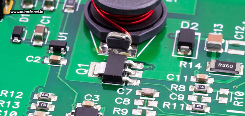
Boost converters, or better known as step-up converters, are the simplest types of DC-to-DC switch mode power converters, used to step up a voltage from the supply to the load. It consists of a diode, a transistor, and a capacitor/inductor. But, the effective working of a boost converter is significantly decided on the kind of PCB used. The way the PCB is designed highly determines how a boost converter performs its function. So, how can we make a good PCB design for such a device?
Creating a good design – three basic steps
One of the easiest methods is to copy the boost converter’s configuration from its figure or testing panel. But, the design may or may not be compatible with the system board, which is why a certain number of steps are to be performed.
First, the output capacitor should be placed and routed in the correct location. The outer transistor should be located near the integrated circuit, linked with a short and large trace to reduce excessive current, because the current flow through the outer transistor is of the pulse type.
Second, the inductor’s copper in the node should be designed in such a way that the high current is managed to take up the least amount of space. It is very important to keep every signal of a sensitive node at a safe distance.
Finally, the input capacitor, which is responsible for controlling the inner circuit and under-current circuit, should be designed such that its ground node and the integrated circuit’s control ground pin are kept nearby. The power ground of the boost converter is made up of the input transistor’s ground node, outer resistor’s ground node, and the integrated circuit’s ground pin. With the input capacitor’s current remaining constant, the distance between the inductor and input capacitor’s node is insignificant.
Also note,
The digital and logic modules are used in small-signal parts. For instance, the resistors and capacitors for the pin are small-signal analog elements for the boost converter. The pins may have a high input impedance, which makes noise particularly sensitive to the power devices and routers. If the trace is route too close to the node, the noise can cause problems by coupling to the pins. Thus, the modules’ ground node and the integrated circuit’s pin should be joined to the integrated circuit’s power ground with a point. There isn’t any high voltage current flowing vis this signal ground, but the noise coupling into the control circuit may result in poor output voltage management, or any other issue.
With all these basics and fundamental ideas, the best PCB can be designed for a boost converter. Miracle Electronics can help you with excellent services related to all types of PCBs for all kinds of applications. You could choose from standard off-the-shelf PCBs, or have special customized PCB assembly manufacturing from India done here, no matter what the size of your project – large, medium, or low. And, rest assured that whatever you choose, you’ll always get only high quality optimal results and cost-effective products at Miracle Electronics.
