
PCBs are one of the integral components of every electronic device and appliance today. From the smartphones and computers that we use every single day to the refrigerators, microwaves, televisions, and other appliances that we can’t do without in our regular lives, PCBs play a very important role. Now, in this blog, let us see how these tiny, yet so functional, PCBs are made that can take up such huge responsibilities of functionalities of the smallest to the largest appliances.
Designing
The first step to manufacturing a PCB is designing. PCB manufacturers use complex software to design circuit boards, which needs to match the function of the PCB prototype. A computer aided design system is used with PCB software installed to lay out the circuit pattern on the board. Once the design is approved, it is exported into a format that the manufacturer uses. The prototype then undergoes checkpoints by software using sophisticated algorithms in order to check that no error goes undetected. A special printer is then used to print out a film that images the PCB, wherein a precise plastic sheet and photo negative of the design are produced.
Printing
The printed design is used to map out a figure of a copper path. The board is then laminated to receive the copper, providing the board with substrate material to make it dust-resistant. The laminate is then cleaned before layering it up with a photosensitive film. The prototype is then blasted with UV light to harden the copper underneath the resist, while ensuring that the copper parts that do not need to harden are avoided. The unwanted copper is then removed, and the prototype is examined to ensure that there are no errors.
Layer alignment
All the layers by this time are cleaned and ready to be aligned. The layers are them placed into an optical punch machine to punch the required holes. Any error in this position is unable to be corrected, which is why it is important to clear off any errors in the previous step. However, the machine uses a laser to scan the layer and notify if there is any inconsistency with the original Gerber file. If the layers are found to be consistent, they are fused together in a two-part process – layer up and bonding. Then, the holes are bored into the stack board with the help of computer controlling, so that the PCB is precise.
Copper deposition
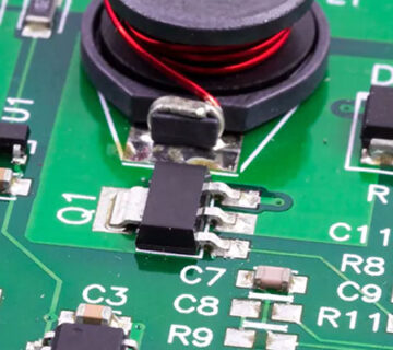
Once the layers are fused together, they are then cleaned in several chemical baths, where thin layers of copper are deposited into the holes. Then, the outer layer is fitted with a photoresist, before it is hardened with UV lights. The unwanted photoresist is then removed, after which a thin layer of copper is applied on the board, where the exposed sections of the board receive copper electroplanting. The board is then given a tin bath to protect the copper during etching, where the unwanted copper is removed to clearly show the conducting areas and connections.
Solder mask application
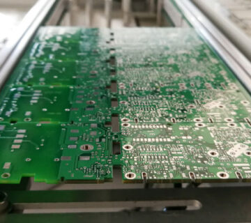
Next, the panels are cleaned and baked in an oven to cure the solder mask. The PCB is then chemically plated to add extra solderability to the board. Hot air-leveled pads may also be used to result in uniform pads, leading to a surface finish. Ink-jet writing is then used on the surface to indicate all the important information on the PCB before the prototype is finally tested. An electrical test is then done to confirm the functionality of the board and its conformance to the original design. Once tested and proved to be absolutely fine, the board is then cut off from the original panel, ready to be used.
You can see how complex and intricate the PCB manufacturing process is. It thus requires a lot of practice to achieve high quality boards. That’s why you need to choose an experienced and professional PCB manufacturer that can be trusted to build the best quality PCB assembly from India so that you can maintain high quality products.