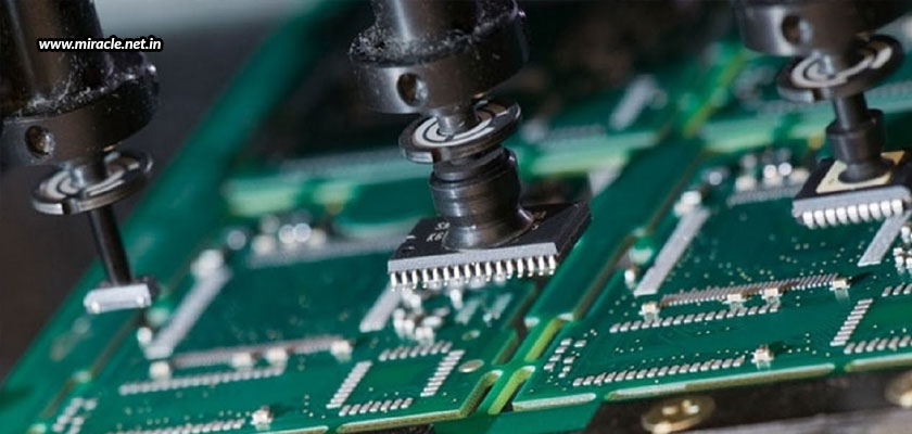
With the PCB being such a complex device, it is important that every tiny component in the circuit design must fit in well within the physical boundary of the board, while being correctly in place to make the right connections, and hence function properly. There could be a hundred components to be placed on a single board, which is why you need an expert manufacturer to build your PCB assembly, so that any kinds of mistakes and errors can be avoided. Miracle Electronics is one such manufacturer who is well-versed at manufacturing even the most complex PCB assembly from India, whether it is a μBGA or a surface mount assembly.
Let us take a look at how such multiple tiny components are placed onto a board. Although the PCB layout process is a complicated and overwhelming procedure, we’ve broken it down into multiple steps so as to split up the complex task into multiple manageable pieces.
Step 1 – Considering the placement
Before beginning any procedure, it is important to plan up well. Same is the case with PCB component placement. You need to understand very well where and how each component needs to be placed. You also need to identify the mechanical constraints on the component location, such as the location of the connectors, the locations of heat sinks, the keep-out zones, etc. Also, the perimeter of the board must be kept free to give enough space for gripping the PCB during assembling, and room to score smaller boards to allow them to be removed from a larger multi-arrayed panel. A good recommendation is to keep all components at least 0.050” from the PCB edge. Further, taller and more fragile components should be kept at least 0.125” from the edge to prevent damage and allow room for tooling access when the board is routed or scored from the panel. Another important aspect to consider is to simplify routing and grounding in a way that the noise between power components, high-speed digital components, and analog components is minimized. Also, the power supplies and associated components should be grouped together, as far as possible from noise-sensitive section of the circuit.
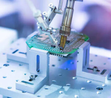
Step 2 – Locating active components
The next step is to located the active components on the board, such as the BGAs, quad packs, and other large high pin count components. It is the room needed to fan out the pin counts that drives the locations of all the components around them. Thus, the active component ICs need to be aligned with the #1 pin or A1 pin in the same orientation, so that the inspection and debugging of the initial prototypes becomes less frustrating.
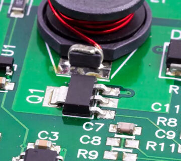
Step 3 – Locating passive components
Once the active components are in place, the next step is to locate the passive components on the board. The bypass or decoupling capacitors on the power pins should be located as close to the IC as practical to minimize the parasitic inductance. The lowest value capacitor should be placed closest to the power pin. The bypass capacitors should be located on the opposite side, directly under the power pin. And, each power pin should have its own bypass capacitor. The polarized components like electrolytic capacitors and diodes should be arranged such that they all face in one direction. Lastly, the inductors should be placed apart, because placing them too close together can cause inductive coupling, changing their value, thanks to their property of generating magnetic fields.
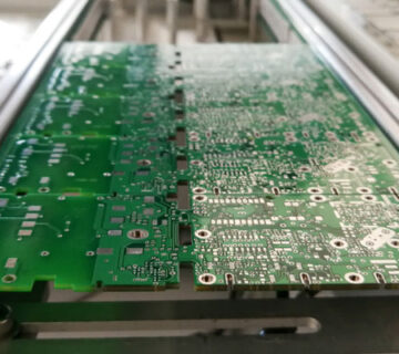
For double-sided boards
When you’re thinking of designing double-sided PCBs, it is recommended to place the lighter and more heat resistant components on the bottom side. This is because double-sided PCBs have to pass through the reflow oven twice. Moreover, the larger components at the bottom need to be glued to keep them from falling off. The smaller passive components cannot be glued, but the surface tension of the solder holds them in place during the second pass through the oven.
These are some very basic guidelines to help with the right component placement on a PCB assembly from India. But, for more complex and distinctive kinds of PCBs, you must always have an expert PCB manufacturer partnered to ensure that the product is appropriate for the application, and thoroughly reliable.