As we all know how important PCBs are in the world full of electronics today, we also know that copper is one of the main ingredients of any PCB. Generally, the thickness of copper used in a PCB is around 35 μm. But, when the thickness of copper used in a PCB ranges from 100 to 400 μm, it is considered as a thick copper PCB; and such PCBs are used for large high current outputs and optimization of thermal management. The thick copper layer allows large PCB cross-sections for high current loads, and encourages heat dissipation.
Design and structure of thick copper PCBs
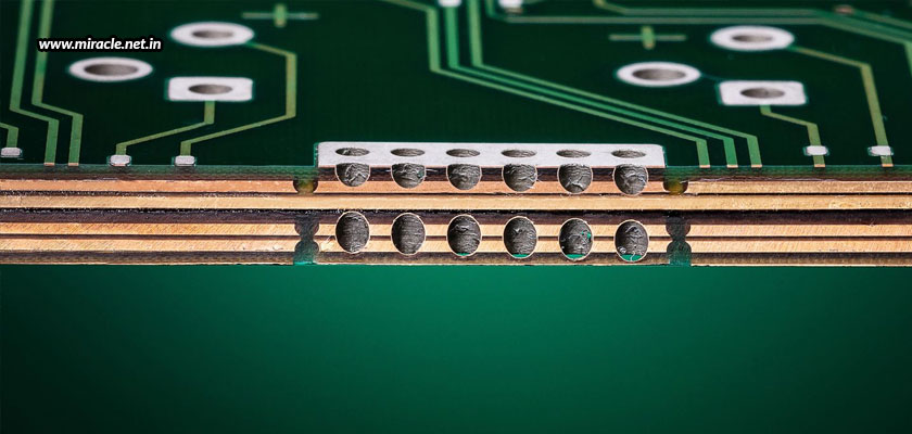
Thick copper PCBs are multi-layered or double-sided, with the technology used making it possible to combine fine layout structures on the outer layers, and thick copper layers in the inner layers. The copper weight combined with an appropriate substrate and thick plating in through-hole circuit makes these thick copper PCBs a reliable wiring platform. Various kinds of etching and plating techniques can be used to manufacture these PCBs, with the main goal being to add copper thickness via plated holes and sidewalls.
Performance of thick copper PCBs
Thick copper PCBs have the best elongation performance, and are not limited by the processing temperature. They can thus be used in hot melt welding methods like oxygen blowing at high melting points. Also, they are not brittle at low temperatures. Even in extremely corrosive atmospheric environments, these PCBs from a strong, non-toxic protective layer. The other benefits that come with thick copper PCBs include high thermal endurance and resistance, excellent current carrying capacity, high mechanical strength, and elimination of complex wire buss configurations.
Applications of thick copper PCBs
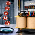
Because of all the above performance benefits that thick copper PCBs offer, they are widely used in various applications such as household appliances, medical applications, and military grade products. With all these performance outcomes, thick copper PCBs offer their applications a long service life, and size reduction of the electronic equipment. The most common applications of thick copper PCBs include solar power converters, torque controls, safety and signal systems, power line monitors, UPS systems, rail traction systems, protection relays, storage pumping plants, overload relays, and HVAC systems.
To summarize, reliable performance and excellent thermal management are two main factors that drive the demand of thick copper PCBs. Today, circuits are built to pass heavy current, meaning that very high heat is produced. Thick copper PCBs help to dissipate heat produced efficiently, thus ensuring optimum performance of the circuit. These are the reasons that in spite of the high prices that thick copper PCBs come at, they are yet in high demand.
In spite of all that is mentioned in the blog above, if you are still unsure of the benefits of thick copper PCBs for your electrical applications, you can always approach an electrical expert or a reliable PCB manufacturer like Miracle Electronics. You can have all kinds of heavy duty copper PCBs for all kinds of industrial applications manufactured when you partner with such an expert PCB assembly manufacturer in India.