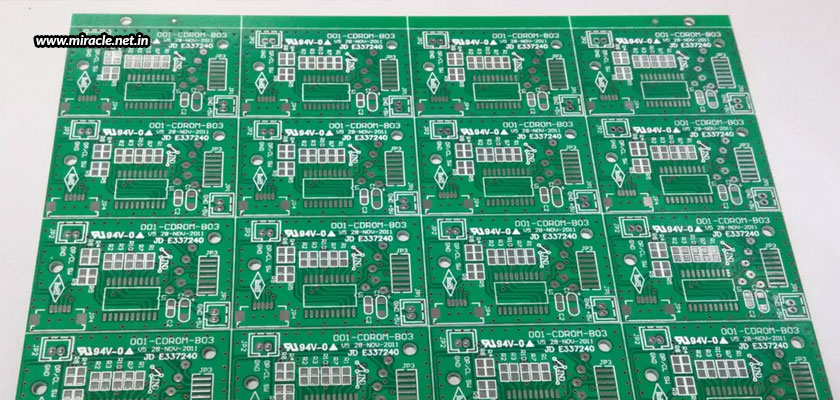
PCBs are an integral part of almost every electronic device and application today; and we all know that, as we may have heard or read the statement multiple times. But, with the challenging times, with everything required to be smart, small, and easy-to-handle, PCBs are required to also be small and light in weight, no matter how high the component density and complicated the design. And, how is that achieved? It’s easy through multi-layered PCBs.
Multi-layered PCBs are multiple layers of PCBs stacked together, with additional dielectric material connecting them as per predetermined standards. A well-designed stack-up can reduce the negative impact of certain factors that hamper signal quality, such as external noise, radiation, impedance mismatch, and signal cross-talk. What we mean by a good stack-up, we’ll explain in the blog below.
How are multi-layered PCBs stacked up?
Multi-layered PCBs are generally built in even-numbered layers, consisting of several different types of layers like signal, ground, and power layers. The most common standard method of stack-up is by beginning with a solid core, and then adding prepreg between cores for inner layers, or between a core and foil for outer layers, such as a 4-layer PCB stack-up. This is followed by a lamination process.
What fabrication options are available?
There are a few options that may be used to fabricate the PCBs, some of them being –
Cap lamination – This process puts the core on the outer layers, and then prepreg in the middle, instead of the general method of beginning with a core and building out using prepreg and foil. However, this is a less-stable lamination process that required the correct tools to be accomplished.
Buried and blind vias – The internal layers are built using foil or cap lamination, with repeated laminated procedures to be executed, in order to capture the vias internally, and complete all the required electrical connections.
Spacing – While considering the materials and compositions on the boards is important, equally important is the spacing that needs to be given between the layers of the PCBs. There are two types of spacing materials that can be used, namely core and prepreg. The core includes copper-plated, glass-reinforced epoxy laminated sheets with a typical thickness between 0.004” and 0.040”; and the prepreg includes a reinforced sheet impregnated with resin with a typical thickness between 0.002” and 0.007”.
To conclude,
A well-designed PCB stack-up and an effective fabrication method used for building a multi-layered PCB can help ensure the right build. Almost every manufacturer uses a set of standard stack-ups, but when you are looking for certain special requirements to be fulfilled, you’ll require a manufacturer who has immense knowledge about every aspect of a PCB so that he can help you with the perfect PCB solution. One such manufacturer is Miracle Electronics, who has resourceful EMS capabilities of product designing, system designing, system architecture, value engineering, manufacturing, and logistics. All these capabilities help Miracle Electronics to deliver a high-quality, consistently-performing PCB assembly from India for every kind of low, medium, and high volumes.