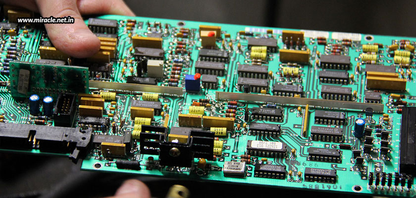
As much as PCB manufacturing is important, equally crucial is testing the PCB. Testing ensures that the product is safe and good to go in every aspect. However, every PCB assembly manufacturer from India has its own different way of testing the product. There are a number of testing procedures available that one can choose from, to analyze the working condition of the components. Let us tell you the most popular ones that are proven and tested across the globe.
In-circuit testing (ICT)
ICT is conducted to check for the placement of the components. The procedure uses an electric probe to be used over a populated PCB to check for factors like opens and shorts, resistance, capacitance, etc. The ICT itself comprises of various individual tests to be conducted on the components. If all these tests are cleared, the PCB is considered to be perfect.
Flying probe testing
This is nothing but a fixtureless ICT that is employed for identifying accessibility problems. This procedure is ideal for testing prototypes and mid-volume types. It is performed using a bed-of-nails fixture that can be easily modified on the basis of the PCB assembly design.
Functional testing
This procedure simulates the real environment in which the PCB is expected to perform. One of the most popular forms of functional testing is the Hot Mock Up Test that is used in combination with the ICT and flying probe testing to ensure that the PCB assembly is error-free and tough.
Boundary scan testing
This procedure is performed for testing wire lines on a populated PCB to analyze pin states in integrated circuits and to measure and analyze the shocks.
Optical microscopy testing
This procedure is used for detecting defects and faults in the PCB assembly, using a high power microscope. Each component is divided into several micro-sections, each being tested under the microscope. The procedure is combined with micro-sectioning to ensure the valid performance of the sample.
Metallographic preparation
This is the cross-sectioning or micro-sectioning analysis. It is conducted to investigate components, opens, shorts, thermo-mechanical failures, etc. In this procedure, a 2D section is removed from the PCB and placed in an epoxy resin, left to solidify. Once it solidifies, the component is receded and exposed. This exposed component is then compared to other non-faulty components using optical microscopy.
Contamination testing
PCB can be contaminated due to a number of elements like chemical reactions, flux residues, improper handling, etc. This makes contamination testing very important. In this process, the PCB is immersed in a solution for a certain time period. If there are ionic contaminants present, the solvent’s constitution will change.
Tin whisker testing
When tin is used as a finishing material on the PCB, it grows into whiskers, which may conduct electricity and affect the operation of the application. In this procedure, the whiskers are corrected using conformal coating; or the tin finish is replaced with metal.
All these testing procedures have their own benefits. When you get in touch with an appropriate PCB assembly manufacturer, you may ask them about the testing method they use, and the benefits achieved from it. Miracle Electronics is an experienced and skilled PCB assembly manufacturer from Germany who has, other than expert manufacturing capabilities, test fixture designs consisting of lab view functional test fixtures, designed for specific PCB assembly testing requirements.